PCB Buisness card with NFC
A clean and sober electronic buisness card with QR-Code and NFC support.
I was browsing through various DIY embedded projects online when I stumbled upon a fun idea: making a business card directly out of a PCB. The interesting part is that a PCB allows you to add interactive features, making it far more engaging than a regular paper card. Once you start searching for PCB business cards, you quickly discover plenty of creative examples and unique designs.
Among all the ideas, the one that stood out the most to me was integrating an NFC tag. This way, people can simply tap the card with their phone to open a website or import contact details automatically. Here’s an example that inspired me : https://www.instructables.com/PCB-Business-Card-With-NFC/
The project itself is fairly straightforward, and since I had a free weekend ahead, I decided to speedrun the whole thing in just two days.
Here’s what I needed to do:
- Design the PCB with all my contact details printed on the silkscreen
- Add an NFC chip with energy-harvesting capability, plus a matching PCB antenna
- As a bonus, include a QR code leading to my personal links
Creating the PCB
As usual, I used KiCad for both the schematic and the PCB layout. The first decision was the card format. I wanted it to fit comfortably in a wallet, so I followed the standard credit card size: ISO ID-1 (85.60 × 53.98 mm). For thickness, thinner is better but manufacturing options and cost also matter so I will choose it when ordering the PCB.
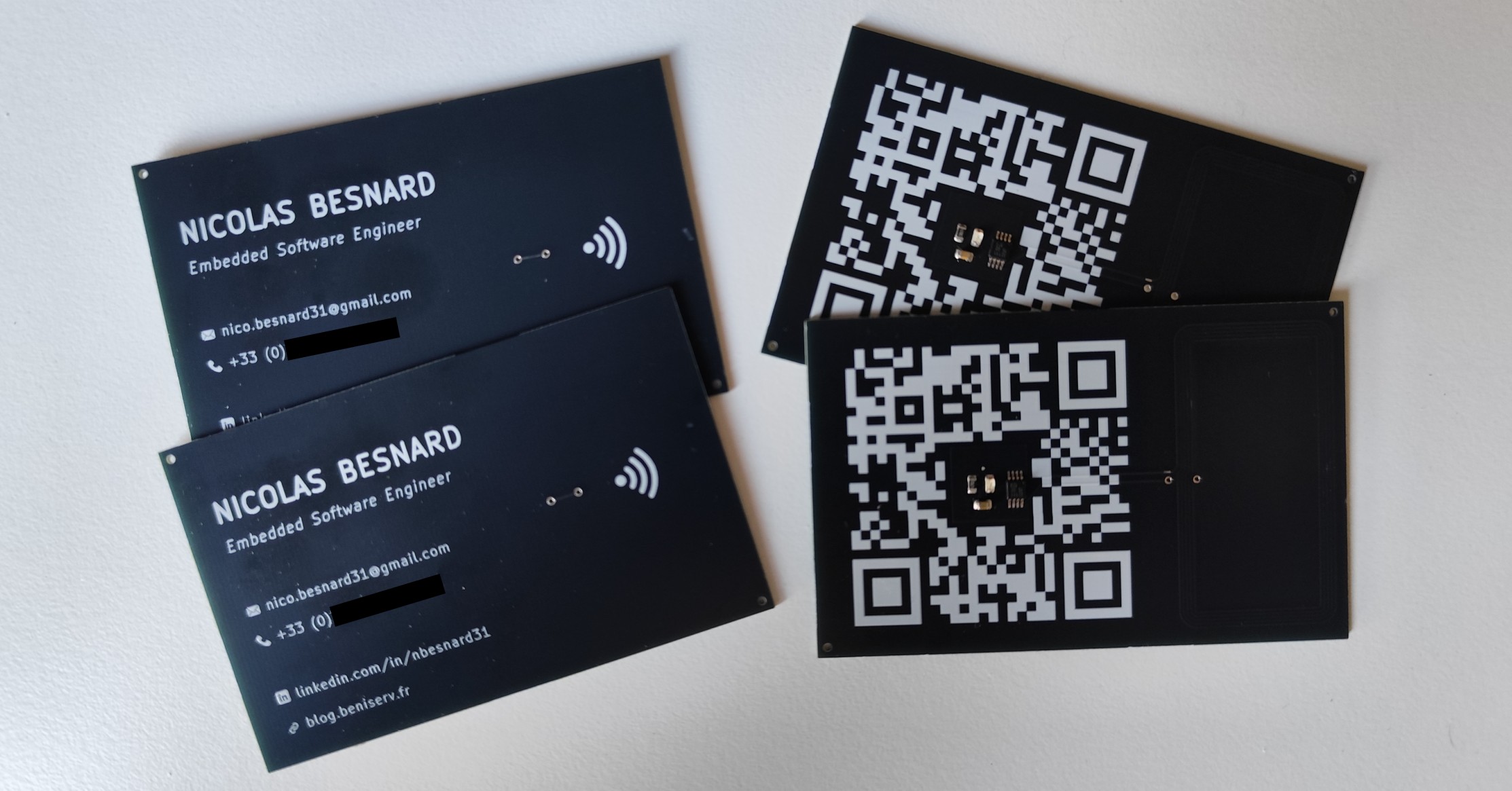
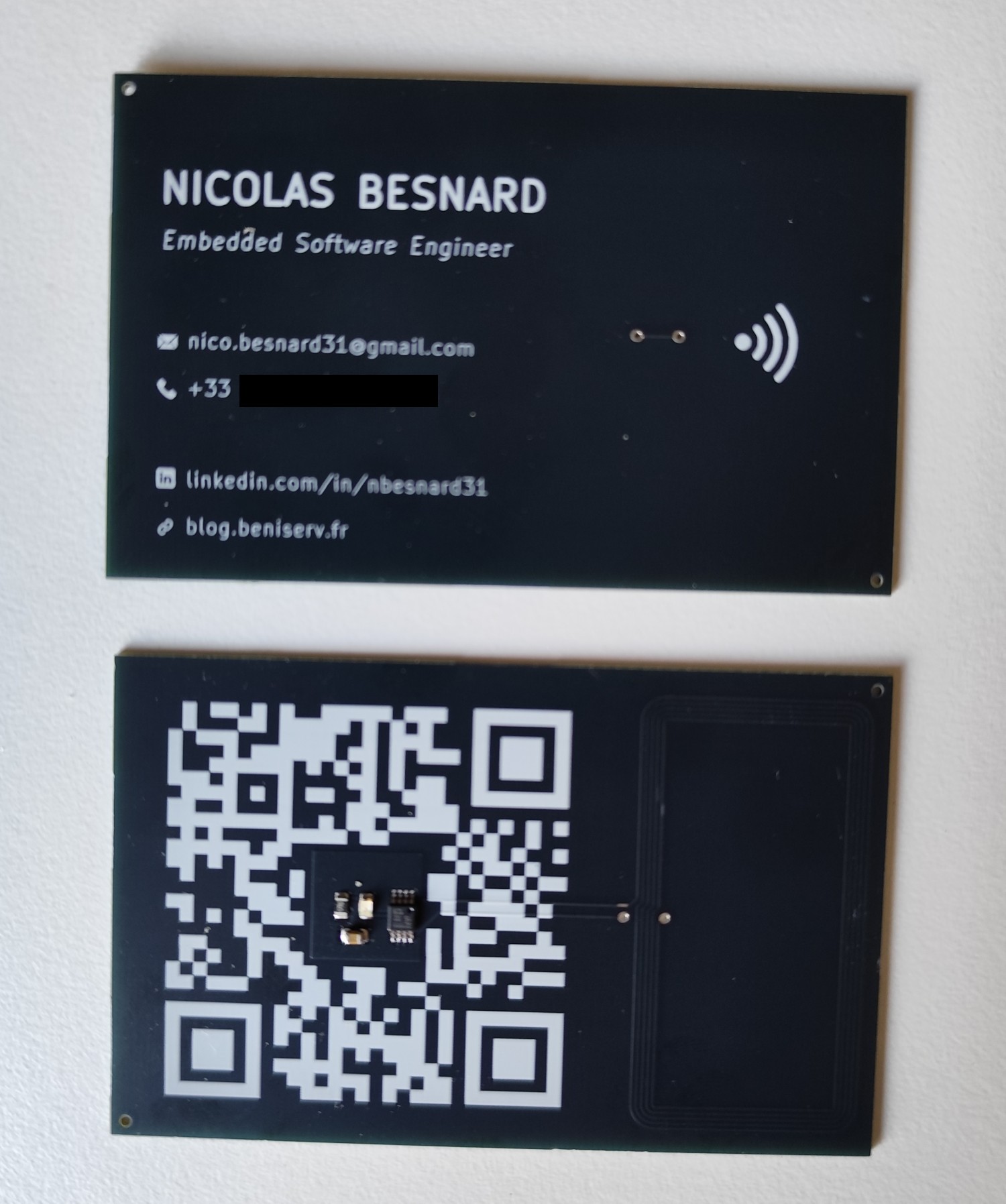
Once the outline was defined, I added all my personal information (name, job title, email, phone number, social links) on the top side, keeping the layout simple and clean. I didn’t want the front to look cluttered. I also added a small NFC “wave” icon to indicate that the card supports tap interaction.
 PCB Top Side
Adding NFC capability
Most of the work of this project is on the bottom side of the PCB, where I integrated the NFC circuitry and antenna.
But first, let’s resume quickly what NFC is.
NFC technology
NFC (Near Field Communication) is a short-range wireless technology that allows two devices to exchange data when they are only a few centimeters apart. It operates at a frequency of 13.56 MHz.
For example, an NFC-enabled smartphone can simbly be brought close to another NFC-capable device to read or write small pieces of data.
 NFC Technology
NFC is particularly useful for embedded devices because the NFC field generated by the NFC reader is enough to energize a NFC tag and so it requires no external power while being read.
NFC IC
To make things easier, I wanted JLCPCB to handle the assembly, so I browsed their component library and only considered chips they already had in stock. I selected the NT3H2111W0FTTJ from NXP because it supports energy harvesting, meaning it can power itself directly from the NFC field without needing a battery.
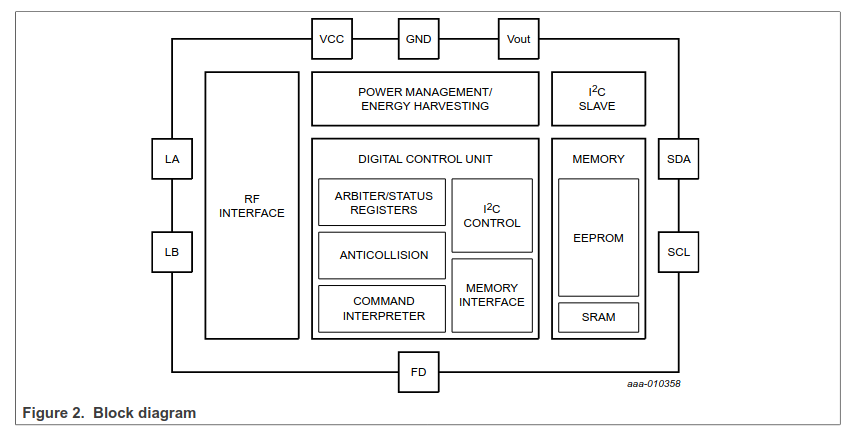 NT3H2111 Block Diagram
As you can see on the block diagram above, it exposes eight pins: :
- LA/LB for the antenna.
- VCC/GND for power.
- VOUT for harvested output voltage.
- SDA/SCL for I2C interface.
- FD for field-detection.
Since I only needed a passive NFC tag containing static data (a URL), I didn’t need I2C communication or field detection, so those pins remain unconnected.
To power the chip, I simply tied VCC and VOUT together, relying entirely on the energy-harvesting feature.
I also wanted a small LED to light up when the card is scanned. With roughly 3 V available from VOUT and using a C84256 LED (2V forward drop, ~20mA forward current), I calculated the series resistor:
Then to power the chip (VCC/GND), we can use the energy harvesting capability by connecting VCC and VOUT together.
\[R = \frac{V_{CC} - V_{LED}}{I_{LED}} = \frac{3 - 2}{0.020} = 50\Omega\]So I used a 47Ω resistor.
The datasheet also recommends a 150–220nF capacitor between VOUT and GND to stabilize the harvested voltage during RF modulation.
All of this is summarized in the datasheet’s example circuit:
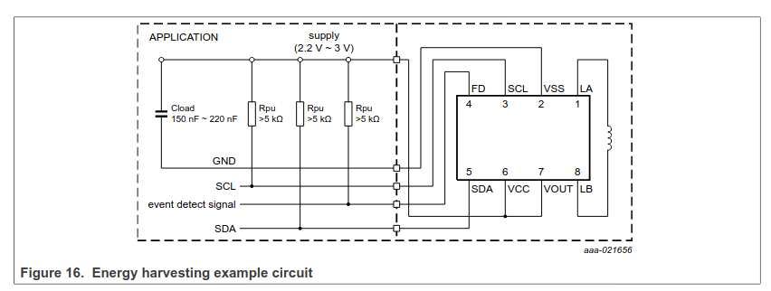 Energy harvesting example circuit
Here is the final schematic I used:
 PCB Buisness Card Schema
NFC Antenna
To operate, the chip needs an antenna. Instead of using an external coil, I used a PCB loop antenna with the correct inductance. Calculating this manually involves several geometric parameters (trace width, spacing, number of turns, etc.).
Fortunately, NXP provides ready-to-use Gerber files for reference antennas compatible with their chips, available in application note AN11276. The matching will probably be far from optimal but for a simple buisness card it doesn’t really matter. So after converting the Gerbers for KiCad import, I simply placed the antenna on my board and connected it to LA/LB.
I just have to keep in mind one important rule: do not place any ground or power plane under or above the antenna, otherwise the magnetic field is blocked and the NFC tag becomes unusable.
 PCB Buisness Card
Adding QR Code
As you maybe noticed, I also included a QR code on the bottom layer so people without NFC can still access the link. The LED sits in the center purely for aesthetics.
I generated the QR code using https://www.qrcode-monkey.com, pointing it to one of my custom subdomain : qr.beniserv.fr.
Since the URL redirects through my domain, I can change the final destination at any time, even after the PCB is manufactured.
Manufacturing
 PCB Buisness Card 3D Render
Once everything was ready, I ordered the board from JLCPCB, who I’ve used many times before. I also asked them to assemble the NFC components, providing them with the BOM and placement files. The excellent KiCAD plugin for JLCPCB generated all required files automatically.
I selected a black PCB finish for a clean, professional look. For thickness, I wanted something close to a real card but without extra manufacturing cost, so 1 mm was the best compromise.
JLCPCB also required the addition of two tooling holes so the PCB could be properly secured during assembly.
All the KiCAD project and fabrication files for this project are available https://github.com/nicopaulb/PCBBuisnessCard.
About two weeks later, the boards arrived. I programmed the NFC tag using the NXP TagWriter app on Android, writing all my contact informations (name, phone number, mail adress and website).
 PCB Buisness Card Photo